|
| OUR RESEARCH ACTIVITIES |
11.jpg)  
We are conducting researches on materials science for innovations in next-generation electronic devices which are expected to contribute to achieve more energy-efficient society. The research topics are includin g the control of physical properties in the nanometer-region nearby the interface of device materials (nano-space functionality research) and the development of the novel materials and technologies required to achieve high-performance devices. Currently, we are mainly focusing on the following research issues.
< Our research activities are introduced in the university's PR magazines!
>
 An interview with Professor Kita is on "Student-edited UTokyo Faculty of Engineerig PR Brochure Ttime!" 2022 summer edition, which is a message to undergraduate and high school
students who are about to choose their carrier paths. An interview with Professor Kita is on "Student-edited UTokyo Faculty of Engineerig PR Brochure Ttime!" 2022 summer edition, which is a message to undergraduate and high school
students who are about to choose their carrier paths.
( Link for "Research on Semiconductor Devices for High-Efficiency Power Conversion"
in Ttime! 2022 summer edition)
An article to introduce professor Kita's work is in "FRONTIER SCIENCES" section on Graduate School of Frontier Sciences PR Magine "SOSEI" No. 40 (published in Sep 2022).
( Link for "Material Science: The Driver of Electron Device Evolution" in
SOSEI No. 40)
 Technologies for Highly Efficient Power Conversion Devices and Their Performance
Improvement Technologies for Highly Efficient Power Conversion Devices and Their Performance
Improvement
Power devices are widely used for every electricity converting process, and their performance directly affects the efficiency of energy usage in the society. Achieving higher performance through innovations in materials and processes is expected to contribute for a siginificant energy-saving. We are focusing on silicon carbide (SiC) devices, which are the keys for reducing the energy loss during power device operation, and conducting researches to achieve dramatically improved performance. In parallel we are also developing the basic technology for gallium oxide (β-Ga2O3) devices, which has recently emerged as a next-generation power device material.
1. SiC Power MOSFET Fabrication Process Technologies
- Novel process technology to achieve high-quality SiC MOS Interface.
- Analysis of MOS interface formation kinetics on SiC to understand the
oxide structures near the MOS interface.
- Understanding of the reactions in SiC surface ~nm region during thermal
processes.
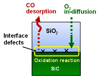
In thermal oxidation of SiC, oxidation-induced byproduct, carbon, is a possible source of the high density interface state density at SiC/SiO2. Thus a smooth elimination of carbon byproduct from the interface is essentially important to form an ideal interface structure. We are currently working on the precise analysis of oxidation kinetics in nanometer-thick region.
 |
|
 |
| ▲ A schematic of SiO2 growth by thermal oxidation of SiC. The reduction
of interface defect formation is needed. |
|
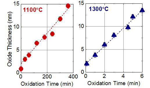
▲ Oxide growth on 4H-SiC(0001) in nanometer-thick region was found to follow
the interface-reaction-limited model (based on accurate determination of
film thickness of nanometer-thick films). |
We have demonstrated the method to reduce the MOS interface state density
to less than 1011 cm-2eV-1 on 4H-SiC (0001) only by thermal oxidation, with the control of the oxidation
conditions to enhance the elimination of carbon precipitations during the
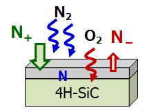
process. In the current industrial processes, a SiC surface nitridation
technique to form a structure where the topmost carbon atoms on the surface
are replaced by nitrogen, is widely employed to suppress the interface
state formation. We are studying the guideline to reduce the interface
level density more efficiently by increasing the reaction rate of nitrogen
on the SiC surface.
 |
|
 |
 |
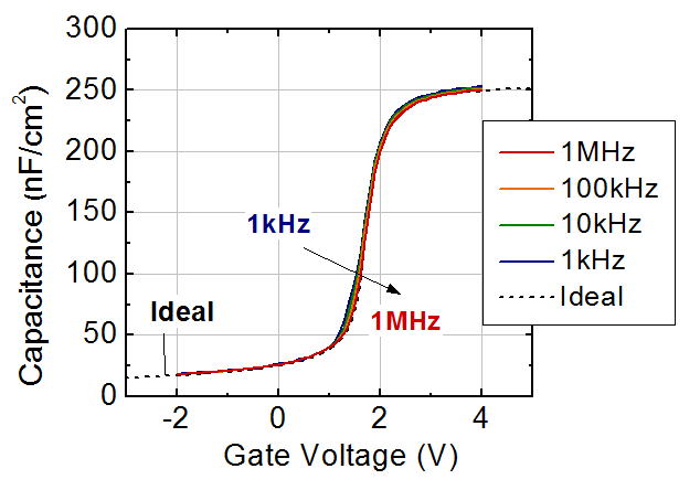
| ▲ C-V (capacitance-voltage) characteristics of 4H-SiC (0001). High-frequency
curve is almost identical with an ideal one shown by dotted line. |
|
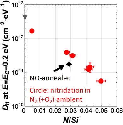
▲ Reduction of interface state density (Dit) was demostrated when the density
of nitrogen incorporated on the SiC surface was maximized based on a reaction
model analysis taking account of both nitridation and oxidation reactions. |
Strained SiOx layer is existing at the interface between the SiC and the
gate insulator SiO2 formed by thermal oxidation. Thanks to the formation
of this interfacial transition layer, the interface with low defect density
is achievable despite of the significant mismatch of the lattice. The analysis
of this interface structure is essential to understand the key factors
that determine the intrinsic properties of the MOS interface.For example,
doping SiO2 with certain elements can change the magnitude of SiO2 strain
in this near- interface region, which is expected to play an important
role for the electrical characteristics of this MOS interface.
 |
|
 |
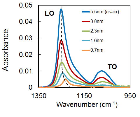
| ▲ Significant peak shifts of lattice vibrations of SiO2 for a few nanometer-thick thermal oxides on SiC, caused by the strained structure formation at SiC/SiO2 interface (FTIR-ATR analysis). |
|
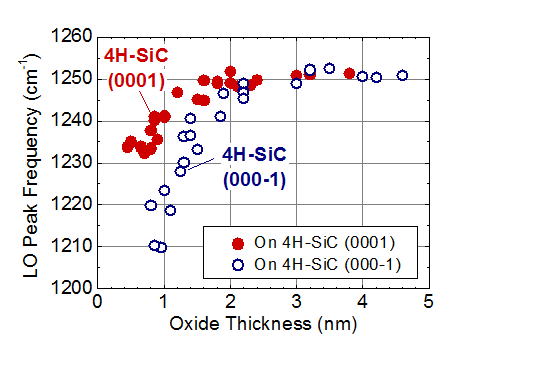
▲Strained structure of thermal oxides on SiC within a few nanometer from
the interface strongly depends on the crystal faces of SiC. We found that
the amount of shift of the lattice vibration peaks is quite different between
the oxides on (0001) and (000-1) faces (thickness-dependence of the FTIR-ATR
peaks). |
2. Study on Gallium Oxide β-Ga2O3 Device Formation Technology for Next Generation
Power Devices
- Development of MOS interface formation technology to realize β-Ga2O3 power MOSFETs.
- Development of SiO2 thin film growth technology on β-Ga2O3 and understanding of the interfacial reactions.
Because of its ultra-wide bandgap, Ga2O3 is expected as one of the next-generation power device materials. In addition to the technology establishment of epitaxial film growth and n-type doping, a large-diameter wafer growth technique by solution growth has been developed especially for β-Ga2O3. Once the high-quality MOS interface formation method is established, high-performance β-Ga2O3 MOSFETs will be available. In our group, the technique to control the SiO2/β-Ga2O3 MOS interface properties are being investigated.
 |
|
 |
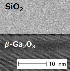
| ▲Cross-sectional TEM image of the interface between β-Ga2O3(001)
epitaxial wafer and a SiO2 film. Atomically flat interface can be formed. |
|
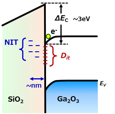
▲ Schematic image of MOS interface with β-Ga2O3 and SiO2. Even though this
is an interace with oxides, they are expected to show a steep transition
from semiconductor to insulator. |
Dielectric Interface Science and Exploration of Novel Dielectric Properties
for the Next-Generation Electronic Devices.
The introduction of new materials for state-of-the-art CMOS and memory
devices is inevitable to innovate their functions. The rapidly spread of
electronics demands a dramatic reduction of the power consumption in the
advanced devices. For example, to drive high-performance MOSFETs with ultra-low
voltages, the gate dielectric formation technology that enables a precise
tuning of the threshold voltage is essentially important. In addition,
the development of the dielectric thin films with novel functions, such
as ferroelectric nanometer-thick films, is strongly demanded to realize
new high-density memories that is operated with ultra-low power consumption.
3. Dielectric Properties and Interface Phenomena of Ultrathin Oxides for Advanced
CMOS Devices
- Material design of high-k (high dielectric constant) oxides for CMOS
gate insulators.
- Understanding the phenomena at oxide interface, such as interface dipole
layer formation which contributes to the advanced threshould voltage control
technology of MOS devices.
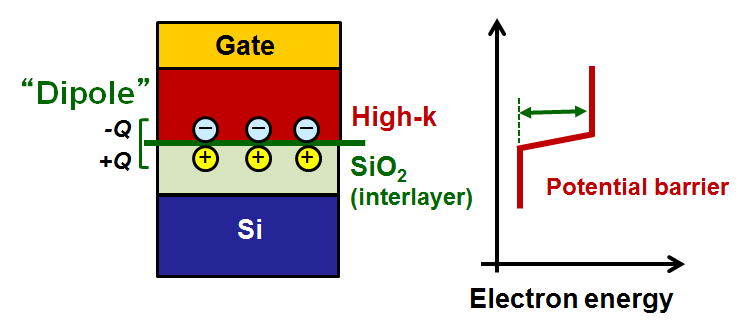
Electron potential barrier sometimes appears at the interface between two
kinds of oxides by "interface dipole effect", even those two
materials are insulators without free electrons. This interface effect
has an important role in MOS devices, for example, in the tuning of threshould
votage of the advanced CMOS devices. We are investigating the physical
origin of the dipoles and developing a guideline for the advanced control
of this phenomenon.
 |
|
 |
| ▲Schematic image of the interface dipole layer between high-k dielectric
and SiO2 on Si (for the case of dipole from high-k toward SiO2). |
|
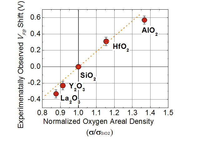
▲ Strength of the interface dipole effect between high-k and SiO2 seems
to correlate with areal density of oxygen atoms in high-k materials. The
microscopic structural property of high-k oxides should be one of the important
factors to detemine the dipole effects. |
4. Material Design of Dielectric Films with Novel Functions Using Atomic Layer
Deposition (ALD) Method.
- ALD growth techniques of high performance nanometer-thick ferroelectric films.
-Understanding of the physical structure and the reactions in the nanometer
region near the HfZrOx/electrode interface.
HfO2 and HfZrOx often show ferroelectricity when they are formed in nanometer-thick
thin films, which is expected to enable the next-generation ferroelectric
devices. The ferroelectricity originates from the orthorhombic phase HfO2
or HfZrOx crystals formed in the film. Therefore the remanent polarisation
exhibited by the films are significantly influenced by their crystallinity.
We employ ALD method to design the stacking structure of the thin films
and to control the growth process as well as the crystallization process
during a heat treatment. We also found that the stresses applied to the
thin films and the interfacial reactions between the electrode and HfZrOx
are one of the important factors to affect the ferroelectricity. For example,
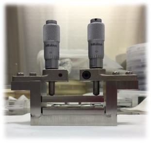
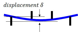
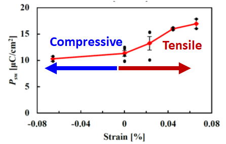
we have found that the change in remanent polarisation when mechanical
strain is applied. We also found that the reactions at the electrode interface
is directly affect the degradation phenomenon of the ferroeletricity.
 |
 |
|
 |
 |
 |
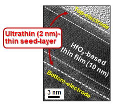
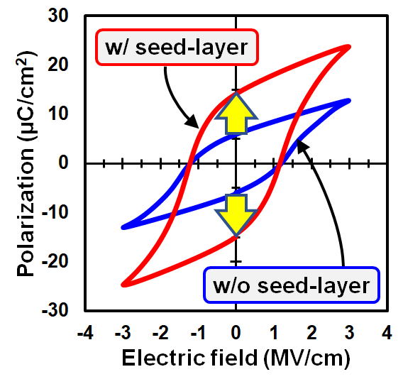
| ▲ Formation of ferroelectric HfZrOx nanofilms by ALD method. Ferroelectricity
can be siginicantly improved by inserting a ultrahin seed layer at the
interfaces to control the crystallinity of the film. |
|
▲Finding of a phenomenon that mechanical stress applied to ferroelectric HfO2 thin films induces a change in the remanent polarisation. |
|
|